Chip Gallery

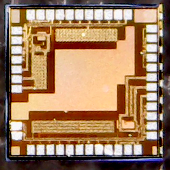
Analog to digital interface circuit for a relative humidity SAW sensor
 

Analog to digital interface circuit for a relative humidity SAW sensor

1-GHz CMOS Differential Ring Oscillator (research project – 2017)


1-GHz CMOS Differential Ring Oscillator (research project – 2017)


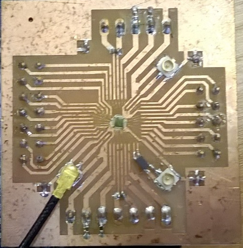
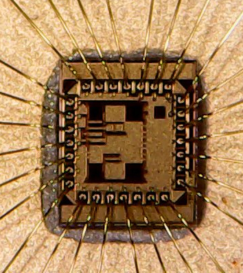
The integrated circuit is a 1-GHz ring oscillator designed in a differential topology, fabricated in theTSMC 180 nm MS/RF CMOS technology. Inaddition to the main oscillator, accessory circuits were included for easiertesting. Notably,anarrowband phase locked loop was included to stabilize the carrier frequency, as well as a 50-Ωbuffer for interfacing with 50-Ωequipment. The purpose of the designed oscillator is to provide a stable signal to a miniaturized wireless power transfer systemenvisaged to supply energy to implanted circuits. The chip was assembled on the surface of aprinted circuit boardusing a FR4 substrate, Ohm). The connections were done with gold wires, using a wire-bonding machine

HBC Transceiver (student project 2016/2017)


 Photo of the HBC Transceiver
(packaged chip assembled in a PCB)
(photo of the die)

High Frequency LC parameter extractor (student project 2016/2017)


Photo of the  LC parameter extractor
assembled on a PCB (wirebonding)

Double Feedback Oscillator (student project 2015/2016)


DF_chip_2016
Double Feedback Oscillator.

Class-E Power Amplifier (student project 2016)


PA_chip_2016
Class-E Power Amplifier.

25-dBm 1-GHz Class-D Power Amplifier (student project 2015)


PA_chip_2015
25-dBm 1-GHz Power Amplifier.

Fully-integrated Tag with Digital Memory (student project 2016)


chip_Juan
Fully-integrated Tag with Digital Memory.


CMOS fully-integrated receiver for medical implants (student project 2015)


chip_FRiano
A CMOS fully-integrated receiver for autonomous implanted devices.


Automatic test and correction of LC resonator (student project 2015)


chip_Negresistance_PSilva
The correction of the LC resonance frequency is done with an ultra-fast a simple circuit based on high dynamic range negative-resistance circuit.


Conditioning circuit for ISFET-based sensor (research project 2014)


 chip_MScRonaldo   
A conditioning circuit that consists of a current-controlled oscillator for ISFET-based sensors, such as glucose. This work was done in collaboration with UNICAMP:
http://www.namitec.org.br/noticias-namitec/199-pesquisa-desenvolve-circuito-de-ultrabaixo-consumo-para-sensor-eletroquimico


400 MHz Superregenerative receiver (research project 2014)


    SR_chip_2014
400 MHz superregenerative receiver for WBAN applications.

2.4 GHz  CMOS Hartley oscillator (student project 2013)


Ultra-low power CMOS oscillator based on the Hartley topology. This project was developed by graduate students as an assignment of the Radio Frquency Electronics course


900 MHz UHF Energy harvester (research project 2012)


This 900 MHz UHF Energy harvester is going to be used for powering a WBAN temperature sensor.


A Duty-Cycle Controlled Variable-Gain Amplifier for WBAN applications (student project 2012)


IMG_1084  A Variable-Gain Amplifier (VGA) whose architecture is based on the superregenerative concept applied in the RF receiver created by Armstrong back in the 1920’s. This technique allows to control the gain by adjusting the duty-cycle of a digital clock. In this way, the complexity for implementing an automatic gain control circuit is reduced, since no D/A converter is needed. This project was developed by graduate students as an assignment of the Radio Frquency IElectronics course VGA_Romero2015


Low Voltage LNA (student project 2012)


This LNA is designed to work with 0.6 V using a standard 180 nm CMOS technology. The measured peak value of |S21| is 9.5 dB as it is seen on the right. This project was developed by graduate students as an assignment of the Radio Frquency IElectronics course


Low Power LNA (student project  2012)


This LNA is designed to consume a low power while has a noise figure below 3 dB. The measured peak value of |S21| is 6 dB as it is seen on the right and the measured power consumption is 1.1 mW. This project was developed by graduate students as an assignment of the Radio Frquency Electronics course


A 2.4GHz Cascode CMOS Low Noise Amplifier (student project 2012)


This LNA works at 2.4GHz with 14.5dB voltage gain and 2.8dB simulated noise figure. Powered from a 1.8V supply, the core measured current consumption is 2.76mA. An output buffer was designed to match a 50Ω load and its current consumption is 5.5mA. It was fabricated with IBM 180nm technology.This project was developed by graduate students as an assignment of the Radio Frquency IElectronics course . The figure in the left shows a micrograph of the LNA during tests and the figure in the right shows the S21 curves, measured and simulated.


2.4 GHz Ultra Low-Voltage Oscillator (research project 2012)


This 2.4 GHz oscillator was designed using a zero-VT transistor in a standard 0.13 μm CMOS process. The post-layout simulation results show that the oscillator starts from a supply voltage of 38 mV, consuming 4 uW and with a phase-noise of -91.5 dBc/Hz. The oscillator is based in the classical common gate Colpitts oscillator topology, but with the tail current degenerated into an inductor, and with additional positive feedback provided by a third inductor on the gate.


Low-voltage Super-regenerative receiver at 2.4GHz ( 2012).


A Super-regenerative receiver at 2.4 GHz was designed in IBM 0.13 μm technology to operate with supply voltages as low as 500 mV. This architecture of receivers is well known by its high gain, sensibility and low power consumption. The receiver is composed by a LNA, an oscillator controlled by the quench signal, and a demodulator. The post-layout simulation results in a power dissipation of 1.5 mW, a quench frequency of 15 MHz and a sensitivity of -70 dBm.